
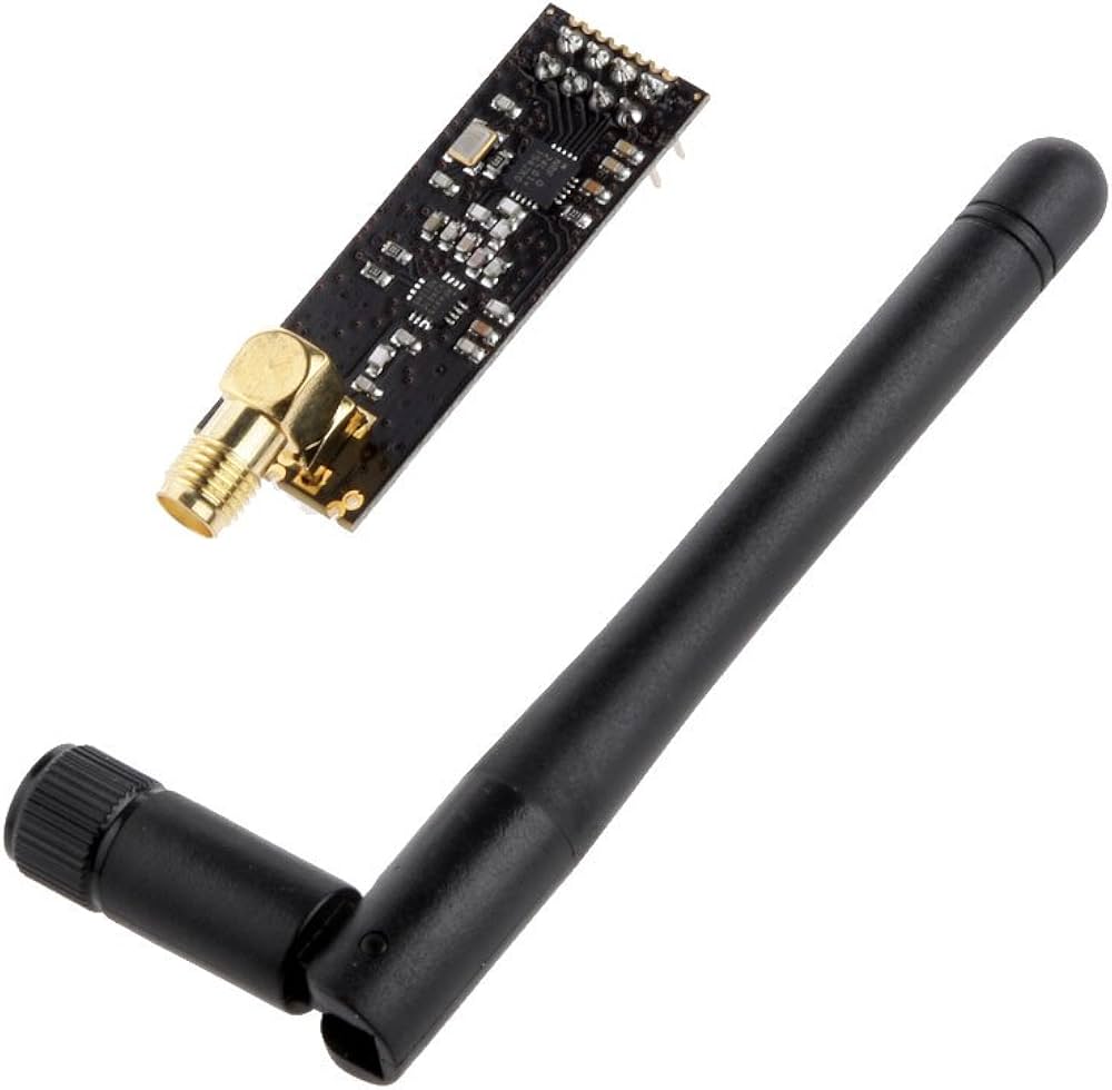
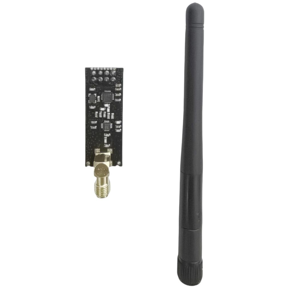
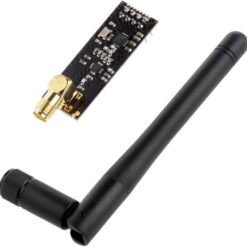
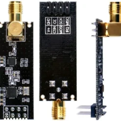
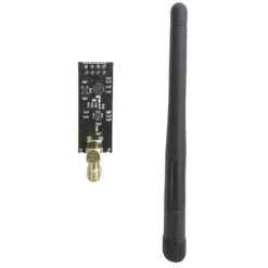
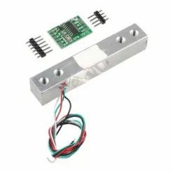
NRF24L01+PA+LNA with Antenna 1100 Meters

₵85.00
The NRF24L01+PA+LNA is the high-power version of the classic NRF24L01 chip, designed for long-distance wireless communication. Thanks to the built-in Power Amplifier (PA) and Low Noise Amplifier (LNA), this module can transmit data up to 1.1km in open areas.
Pro Tip: Power Warning: This module draws more current than the standard version. If you experience connection drops, solder a small capacitor (10µF to 100µF) across the VCC and GND pins, or use a dedicated NRF24L01 Socket Adapter to stabilize the power.
5 in stock
Key Features and Enhancements
This enhanced module differs from the standard nRF24L01+ in several critical ways:
| Feature | Standard nRF24L01+ | nRF24L01+PA+LNA | Enhancement |
| Transmit Power (PA) | Up to 0 dBm (1 mW) | Up to +20 dBm (100 mW) | 100\times stronger signal. |
| Receive Sensitivity LNA) | Standard -82 dBm | Improved approx -100 dBm |
Can reliably detect weaker distant signals. |
| Antenna | On-board PCB or small external whip | External Antenna (usually 2.4 GHz duck/rubber antenna) | Better radiation pattern and placement flexibility. |
| Range (Ideal) | approx 50 to 100 meters | Up to 1100 meters (or more) | Dramatic increase in link distance. |
| Power Consumption | Very Low | Higher, requires stable external power during transmission. | Must be connected via 3.3V and requires a stable power supply. |
Technical Specifications
The module operates on the same core principles and protocol as the standard chip ,but with boosted performance:
- Frequency Band: 2.4GHz ISM (Industrial, Scientific, and Medical) band.
- Data Rate: Supports 250Kbps Mbps, and 2 Mbps.
- Operating Voltage: 1.9V to 3.6V (The nRF24L01+ chip itself).
- Logic Level: 3.3V for all SPI and control pins. Requires a logic level converter if interfacing with a 5V microcontroller like the Arduino Uno.
- Interface: Uses a fast SPI (Serial Peripheral Interface) for communication with the microcontroller.
- Protocol: Supports the enhanced ShockBurst TM= protocol, which handles auto-acknowledgement and packet re-transmission.
Power Supply Requirement
Due to the powerful dBm Power Amplifier (PA), the module has a critical power requirement:
- Current Draw: During peak transmission, the module can draw currents up to 100mA to 150mA
- Instability Risk: A standard 3.3V regulator on an Arduino board (which might only supply 50 mA to 100 mA) is often insufficient and leads to voltage dips, causing the module to reset or fail transmission.
- Solution: It is highly recommended to use an external, dedicated 3.3V power supply or a dedicated power adapter board with an on-board high-current 3.3V regulator and smoothing capacitors to power the module.
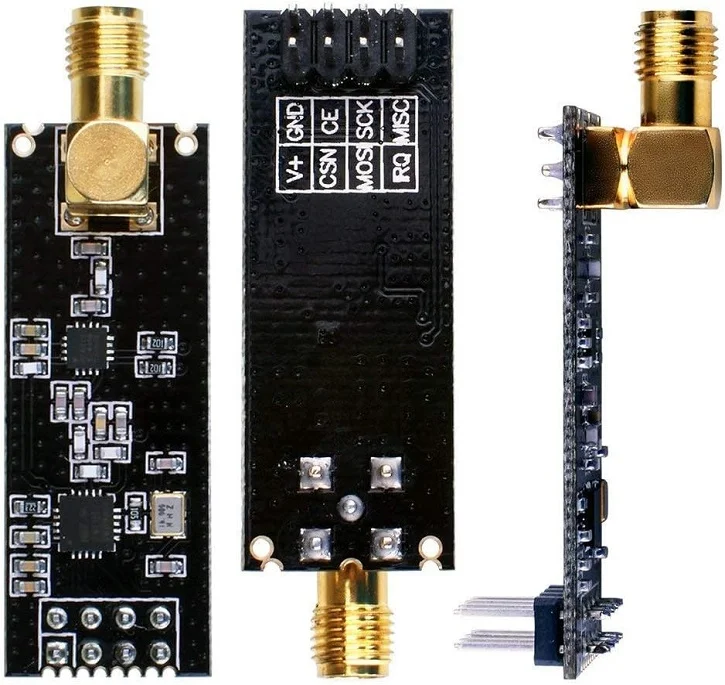
Pinout and Connection
The module uses an 8-pin connector, typically with a 4 header.
| Pin Name | Description | Connection (to MCU) | Note |
| GND | Ground | GND | |
| VCC | Power Supply | Stable 3.3V | Must be clean and high-current. |
| CE | Chip Enable | Digital I/O pin | Toggles between RX and TX modes. |
| CSN | Chip Select Not | SPI CS pin (Digital I/O | Selects the device for SPI communication. |
| SCK | Serial Clock | SPI pin CLK pin |
Clock signal for SPI communication. |
| MOSI | Master Out Slave In | SPI MOSI pin | Data from $\text{MCU}$ to module. |
| MISO | Master In Slave Out | SPI MISO pin | Data from module to MCU |
| IRQ | Interrupt Request | Optional Digital I/O pin | Sends an interrupt signal upon packet completion. |
Be the first to review “NRF24L01+PA+LNA with Antenna 1100 Meters”
Related products


Reviews
There are no reviews yet.